【Exchange Information】The Center for Plasma and Thin Film Technologies invited a PhD student from the Joining and Welding Research Institute at Osaka University to Taiwan for a research and academic exchange
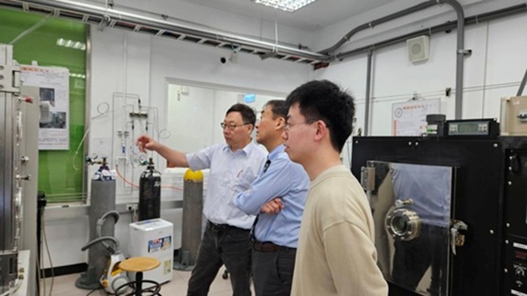
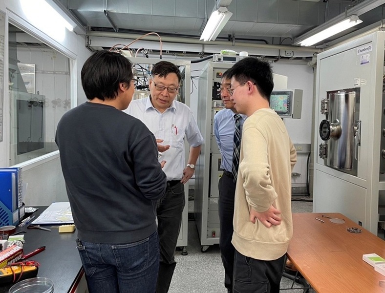
The Center for Plasma and Thin Film Technologies (CPTFT) at MCUT has signed a Memorandum of Understanding (MoU) with the Joining and Welding Research Institute (JWRI) at Osaka University in Japan. CPTFT Director Jyh-Wei Lee and Professor Nishikawa Hiroshi from JWRI studied on soldering tin films. As part of this collaboration, we invited Wang Xinjie, a PhD student supervised by Professor Nishikawa, to Taiwan for research on the fabrication of CoSn3 films with specific orientations. This visit aims further to strengthen the academic exchange between the two universities.
After completing his exchange program in Taiwan, Wang Xinjie stated:He would like to express my heartfelt gratitude to Prof. Lee and Dr. Chia-Lin Li for providing this valuable opportunity for academic exchange, as well as to the other professors and fellow students for their assistance during this period. During my time at the Thin Film Center, He successfully prepared CoSn₃ thin films using the sputtering system. By adjusting the different types of power supplies and working pressure, He achieved preliminary control over the crystal orientation of the CoSn3 thin films.
The experimental results suggest that under DC power mode, employing a higher power and lower working pressure yields CoSn3 thin films predominantly oriented along the (600) plane. Conversely, switching to RF power mode, along with lower power and higher working pressure, favors the formation of CoSn3 thin films primarily oriented along the (312) plane. The variation in preferred orientation can be attributed to the energy of the sputtered particles upon reaching the silicon substrate. Under the DC mode with higher power and lower pressure, the particles possess higher energy, resulting in the densely packed (600) plane. In contrast, lower power and higher pressure under RF mode lead to the formation of the (312) plane.The obtained samples will undergo subsequent testing to determine whether they can effectively control the tin grain orientation in solder joints for electronic packaging interconnects.
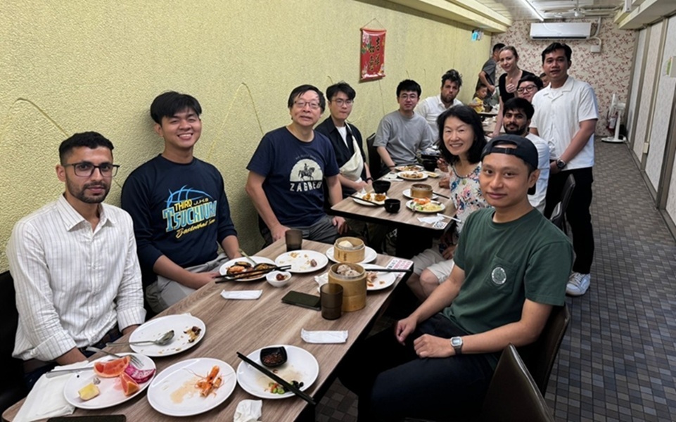
During his two-month exchange in Taiwan for student Wang Xinjie, this experience not only enhanced his academic knowledge in many areas of his field but also led to significant progress in his experimental research. In addition to the academic gains, Wang also formed lasting friendships with Taiwanese colleagues, which made the entire exchange process even more fulfilling and meaningful. The research center's initiative to provide international students with opportunities to visit Taiwan deepens cultural understanding and friendship between nations and promotes the development of more international academic collaborations for the center.
Source: Center for Plasma and Thin Film Technologies


